Future Energy Challenge 2004: Variable Frequency Motor Drive
![]() If you are one of those people that love Assembly, feel free to read
through the PIC18F assembly from the FEC motor drive by clicking on
the icon to the left.
If you are one of those people that love Assembly, feel free to read
through the PIC18F assembly from the FEC motor drive by clicking on
the icon to the left.
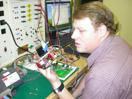
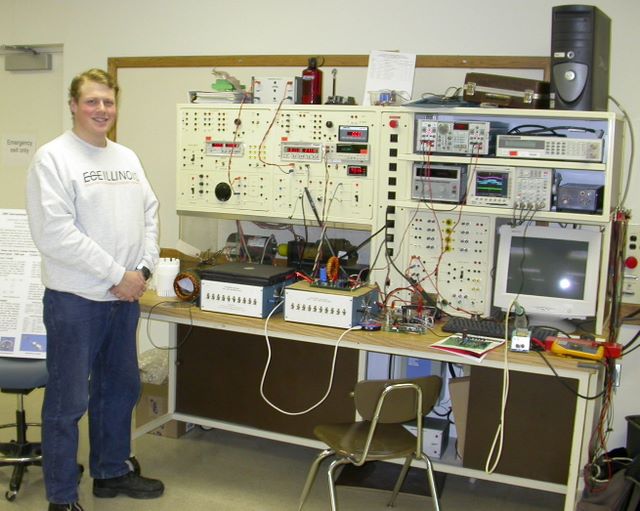 What do I do when I get back from Australia but decide that I want to
know what makes motors go in circles? Enter Future Energy Challenge 2004, a
design competition in which we were soundly trounced by the group from
the University of Belgrade, Serbia. I was in charge of
writing firmware for this project. This photo was taken during Engineering
Open House. On the bench are the PFC, inverter and control, and laptop. We
were spinning a the motor/dyno in the background with it during the whole
demonstration, explaining PWM to groups of pre-college students wandering
around. I really enjoy standing around satisfying other people's curiosity.
You never know when someone else's potentially uninformed question will
make your mind consider something differently. You also cannot ever fully
understand something without having to patiently explain it to someone else.
Like re-reading a paper out loud after it has been written, you pick up a
new understanding of something trying to convey a system's operation.
What do I do when I get back from Australia but decide that I want to
know what makes motors go in circles? Enter Future Energy Challenge 2004, a
design competition in which we were soundly trounced by the group from
the University of Belgrade, Serbia. I was in charge of
writing firmware for this project. This photo was taken during Engineering
Open House. On the bench are the PFC, inverter and control, and laptop. We
were spinning a the motor/dyno in the background with it during the whole
demonstration, explaining PWM to groups of pre-college students wandering
around. I really enjoy standing around satisfying other people's curiosity.
You never know when someone else's potentially uninformed question will
make your mind consider something differently. You also cannot ever fully
understand something without having to patiently explain it to someone else.
Like re-reading a paper out loud after it has been written, you pick up a
new understanding of something trying to convey a system's operation.
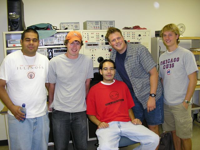 This is a picture of the FEC controls team. These five people were tasked with writing
the software that would make our home-grown variable frequency drive make a home
grown induction motor go in circles. VFD is how you change the speed of induction
motors. You cannot just change the voltage into them, as their speed is based
on the frequency of the incoming power. The best way to change speed is to
somehow change the frequency of the incoming AC waveform. The firmware we
wrote for the PIC 18F series, all 3000 lines of it, accomplished that. I was the only
one on the controls team with any real assembly language experience. I completed
all the course requirements to be a computer engineer
before switching to EE for my super senior year.
This is a picture of the FEC controls team. These five people were tasked with writing
the software that would make our home-grown variable frequency drive make a home
grown induction motor go in circles. VFD is how you change the speed of induction
motors. You cannot just change the voltage into them, as their speed is based
on the frequency of the incoming power. The best way to change speed is to
somehow change the frequency of the incoming AC waveform. The firmware we
wrote for the PIC 18F series, all 3000 lines of it, accomplished that. I was the only
one on the controls team with any real assembly language experience. I completed
all the course requirements to be a computer engineer
before switching to EE for my super senior year.
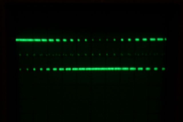 This is what the firmware outputs. This picture is one phase
worth of control signals, that eventually get turned into gating signals for the hex
bridge. If you look at it, you can see that the bright and dark approximates a sine
wave. This photo came out of my digital camera using my personal scope in my apartment.
As you change the speed command to the VFD, the system changes the timing such that
the sine wave approximation goes either faster or slower. These signals are piped
into a bunch of big transistors that turn on and off a high voltage DC source in
alignment with these control signals. By the time this pulse width modulated DC gets through
the inductance of a motor, you have a pretty good looking AC sine wave. We were
using three phase motors and controls, so the control code actually produced three
waveforms like this, all 120 degrees out of phase from the previous.
This is what the firmware outputs. This picture is one phase
worth of control signals, that eventually get turned into gating signals for the hex
bridge. If you look at it, you can see that the bright and dark approximates a sine
wave. This photo came out of my digital camera using my personal scope in my apartment.
As you change the speed command to the VFD, the system changes the timing such that
the sine wave approximation goes either faster or slower. These signals are piped
into a bunch of big transistors that turn on and off a high voltage DC source in
alignment with these control signals. By the time this pulse width modulated DC gets through
the inductance of a motor, you have a pretty good looking AC sine wave. We were
using three phase motors and controls, so the control code actually produced three
waveforms like this, all 120 degrees out of phase from the previous.
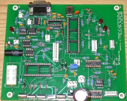
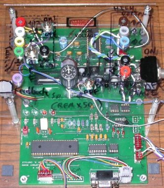 This is the first version of the board that the class produced. At the bottom is the
control board, and at the top of that is the inverter board. To make testing easier,
I mounted a plastic sheet over the top with DC inputs, AC outputs, a speed pot
and programming ports. This was the team's first attempt at PCB layout, and it is,
in a word, a disaster. The first time I tried working on this, I was humming circus
calliope music to myself.
All the bypass caps are in a line, the connectors are all in different directions, there
were no test points that are reachable, even when not mounted under the cover. Layout
is extremely
important in motor drives, and we spent more time fooling around with ground bounce
due to poor PCB layout and ground routing then perhaps any other single problem. It was
after the failure of this that I started working on The Cube, so I could have a more
reliable and robust development platform based on the FEC hardware.
This is the first version of the board that the class produced. At the bottom is the
control board, and at the top of that is the inverter board. To make testing easier,
I mounted a plastic sheet over the top with DC inputs, AC outputs, a speed pot
and programming ports. This was the team's first attempt at PCB layout, and it is,
in a word, a disaster. The first time I tried working on this, I was humming circus
calliope music to myself.
All the bypass caps are in a line, the connectors are all in different directions, there
were no test points that are reachable, even when not mounted under the cover. Layout
is extremely
important in motor drives, and we spent more time fooling around with ground bounce
due to poor PCB layout and ground routing then perhaps any other single problem. It was
after the failure of this that I started working on The Cube, so I could have a more
reliable and robust development platform based on the FEC hardware.
 Following the initial two board solution, which was two separate groups' projects
connected by wires, we get to the first "integrated" drive/control. There is also a separate
large PFC, which is actually quite slick looking compared to this.
This was another persons first PCB layout attempt, and looks like a disaster. The only
good way to learn PCB layout is to do it, and then have someone tell you why your
board looks ugly. This particular board did not work, and is actually quite
humorous to look back on now. There are connectors kind of randomly
distributed, bypass caps all over the place, and my favorite, that
little quasi-arc of LED's in the upper right hand corner, complete
with their current limiting resistors kind of all over.
Following the initial two board solution, which was two separate groups' projects
connected by wires, we get to the first "integrated" drive/control. There is also a separate
large PFC, which is actually quite slick looking compared to this.
This was another persons first PCB layout attempt, and looks like a disaster. The only
good way to learn PCB layout is to do it, and then have someone tell you why your
board looks ugly. This particular board did not work, and is actually quite
humorous to look back on now. There are connectors kind of randomly
distributed, bypass caps all over the place, and my favorite, that
little quasi-arc of LED's in the upper right hand corner, complete
with their current limiting resistors kind of all over.
 This is what the Rev B board looked like when it was under test. The
importance of having connectors in standard places can be seen by
this picture. When debugging boards, it is very handy to be able to
get to the back side without having huge tangles of things all over
the place. I'm not sure I actually worked on this board much, as at this point
I was dragging in The Cube to do firmware stuff, and leaving this mess to
the hardware guys.
This is what the Rev B board looked like when it was under test. The
importance of having connectors in standard places can be seen by
this picture. When debugging boards, it is very handy to be able to
get to the back side without having huge tangles of things all over
the place. I'm not sure I actually worked on this board much, as at this point
I was dragging in The Cube to do firmware stuff, and leaving this mess to
the hardware guys.
 Here's the rev C board. This is an improvement over the rev B boards,
but still not quite there yet- We had trace width issues with this,
and also switched to a different inverter design in rev D which
required a new layout.
Here's the rev C board. This is an improvement over the rev B boards,
but still not quite there yet- We had trace width issues with this,
and also switched to a different inverter design in rev D which
required a new layout.
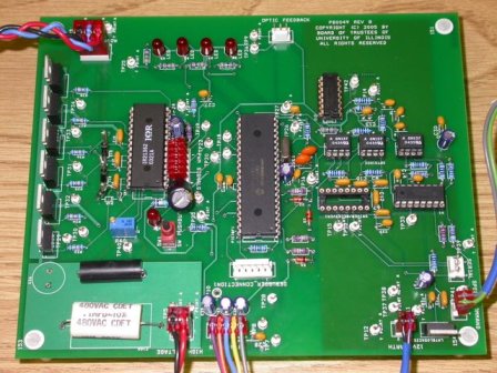
 After getting really annoyed at the Rev C boards, I sat up one night
and laid out another board. This is the rev D board. I attempted to fix
grounding, layout, and isolation issues with this revision. Of course, it
didn't work quite as planned, but at least it looked better. The board
is still very large since
the box, heat sink, and ancillary bits were already designed at this
point. This was my first experience laying out a circuit board. Odd
that as a super senior I would never have done PCB layout before,
but I guess PCB layout is "technician" work and not "engineering"
work. That in spite of the fact that we eventually came to a
consensus that one of the largest problems with this project
was poor signal routing.
After getting really annoyed at the Rev C boards, I sat up one night
and laid out another board. This is the rev D board. I attempted to fix
grounding, layout, and isolation issues with this revision. Of course, it
didn't work quite as planned, but at least it looked better. The board
is still very large since
the box, heat sink, and ancillary bits were already designed at this
point. This was my first experience laying out a circuit board. Odd
that as a super senior I would never have done PCB layout before,
but I guess PCB layout is "technician" work and not "engineering"
work. That in spite of the fact that we eventually came to a
consensus that one of the largest problems with this project
was poor signal routing.
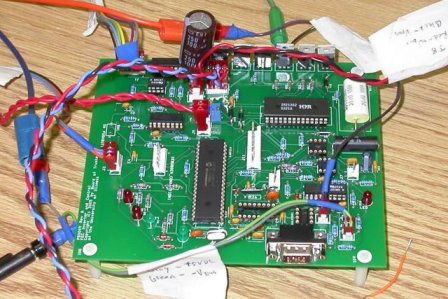
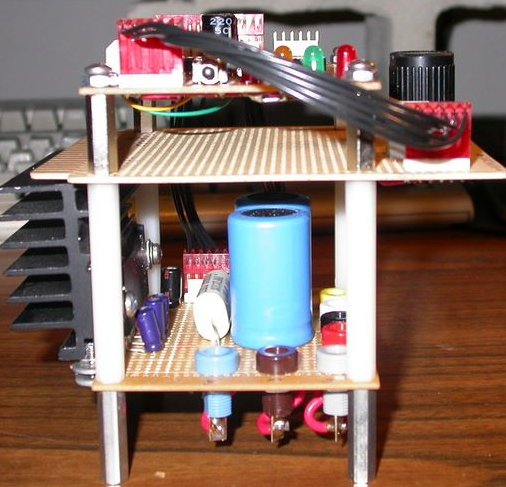 After the debacle trying to debug code on the Rev A board set,
I got fed up and went to my apartment to put together what I
started calling "my hunk of junk". This is a stack of three boards.
The top is the control, middle is the user interface, and bottom
is the inverter. This board stack is what was used to get the
PWM oscilloscope image further up on the page. One of the
main reasons I did this was so that I would have a known-good
thing to whip out when people started saying "It's the software
that is doing this." I could hook this up, put the scope on the
PWM outputs, load the same code and say definitively that no,
in fact, it was not the code that was failing.
After the debacle trying to debug code on the Rev A board set,
I got fed up and went to my apartment to put together what I
started calling "my hunk of junk". This is a stack of three boards.
The top is the control, middle is the user interface, and bottom
is the inverter. This board stack is what was used to get the
PWM oscilloscope image further up on the page. One of the
main reasons I did this was so that I would have a known-good
thing to whip out when people started saying "It's the software
that is doing this." I could hook this up, put the scope on the
PWM outputs, load the same code and say definitively that no,
in fact, it was not the code that was failing.
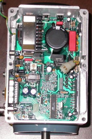
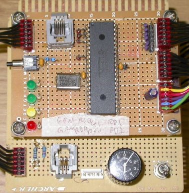 This is the top view of the cube. At left are the status LEDs,
the reset button, the cable to the user interface board, and the
programming port. Along the bottom is the feedback
optical interrupter feedback (Brian wrote a good hunk
of the feedback code, dubbed "bootleg control" by him),
a speed control, and an on/off switch. The right hand
side has two cables that go down to the inverter board,
carrying PWM and control voltages. The multicolored
cable goes to the power supplies that were used for testing.
This is the top view of the cube. At left are the status LEDs,
the reset button, the cable to the user interface board, and the
programming port. Along the bottom is the feedback
optical interrupter feedback (Brian wrote a good hunk
of the feedback code, dubbed "bootleg control" by him),
a speed control, and an on/off switch. The right hand
side has two cables that go down to the inverter board,
carrying PWM and control voltages. The multicolored
cable goes to the power supplies that were used for testing.
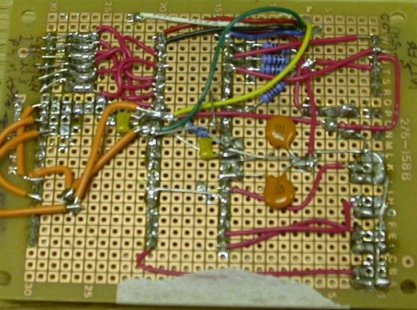 The bottom of the control board. The one big benefit
of wiring up things with these radio shack boards is
that emergency changes are easier than using real PCBs.
The engineer can move wires and slap things down as they
see fit. Of course, the more dense things get, the more
annoying this is, and the easier it is to short things out.
The bottom of the control board. The one big benefit
of wiring up things with these radio shack boards is
that emergency changes are easier than using real PCBs.
The engineer can move wires and slap things down as they
see fit. Of course, the more dense things get, the more
annoying this is, and the easier it is to short things out.
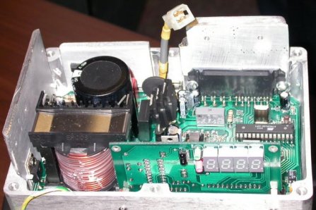
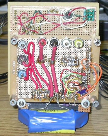 Here's the business end of the cube. DC in at red and
black at the top, AC 3 phase out on the left. The tangle
of wire at the right is the control cable and low voltage
wiring. This worked when ran with an assortment of
bench supplies, but refused to operate when used
with the FEC's PFC and power supply board.
Here's the business end of the cube. DC in at red and
black at the top, AC 3 phase out on the left. The tangle
of wire at the right is the control cable and low voltage
wiring. This worked when ran with an assortment of
bench supplies, but refused to operate when used
with the FEC's PFC and power supply board.
 One of the late night lab sessions attempting to
trace out ground bounce issues. The cube was in
the shop, at the right is a Rev D PCB that we are
attempting to get working. This photo pretty much
summarizes the mood I had toward the end of the FEC.
The ground bounce issue only appeared when we were
running any of our boards off the FEC designed power supply.
The FEC designed power supply worked fine when running
load resistors. Definitely the most annoying problem ever.
One of the late night lab sessions attempting to
trace out ground bounce issues. The cube was in
the shop, at the right is a Rev D PCB that we are
attempting to get working. This photo pretty much
summarizes the mood I had toward the end of the FEC.
The ground bounce issue only appeared when we were
running any of our boards off the FEC designed power supply.
The FEC designed power supply worked fine when running
load resistors. Definitely the most annoying problem ever.
 This is the entry that won, from the University of Belgrade,
Serbia. These guys really had their act together, and
totally blasted the other competitors out of the water.
I'm not sure that this device would be as cheap as it
was purported to be, but it was definitely rock
solid, well-built, and well-engineered. They used
the same inverter section that the other teams did,
but managed to pack all their stuff into a nicely
machined aluminum enclosure. They used an
Atmel microcontroller instead of a PIC, and
more commercially available parts. But theirs
worked, and it worked well.
This is the entry that won, from the University of Belgrade,
Serbia. These guys really had their act together, and
totally blasted the other competitors out of the water.
I'm not sure that this device would be as cheap as it
was purported to be, but it was definitely rock
solid, well-built, and well-engineered. They used
the same inverter section that the other teams did,
but managed to pack all their stuff into a nicely
machined aluminum enclosure. They used an
Atmel microcontroller instead of a PIC, and
more commercially available parts. But theirs
worked, and it worked well.
 Look at this thing! They had an IR port on the
front and an LED display showing RPMs. I learned
several valid lessons from this experience: First off
all, Serbian engineers from Belgrade are a robust
and intelligent group of people. Next, you show a
lot of confidence in your project if you show up
with nothing but a box containing your prototype.
U of I showed up with a car full of tools and test
equipment. The folks from Belgrade showed up
with a single case containing their finished product,
wrapped in towels and bubble wrap. If you feel you
might need a whole portable electronics bench when
it is time to demo your device, then it is too late.
You are not going to impress anyone at demo time
by pulling out oscilloscopes and tracking down bugs.
That just makes you look unprepared to actually
show the thing off.
Look at this thing! They had an IR port on the
front and an LED display showing RPMs. I learned
several valid lessons from this experience: First off
all, Serbian engineers from Belgrade are a robust
and intelligent group of people. Next, you show a
lot of confidence in your project if you show up
with nothing but a box containing your prototype.
U of I showed up with a car full of tools and test
equipment. The folks from Belgrade showed up
with a single case containing their finished product,
wrapped in towels and bubble wrap. If you feel you
might need a whole portable electronics bench when
it is time to demo your device, then it is too late.
You are not going to impress anyone at demo time
by pulling out oscilloscopes and tracking down bugs.
That just makes you look unprepared to actually
show the thing off.

